Srivatsa
Chakravarthi
- Work
- Home
- srivatsa@uw.edu
- Electrical and Computer Engineering
University of Washington
185 Stevens Way
Paul Allen Center – Room AE100R - Seattle, WA
Hi there!
I am final year PhD student working on photonic nanofabrication for quantum technologies. Curiosity drives me to explore, learn and apply. During my graduate studies I have worked on a wide variety of projects. From machining components for my home-built L-He cryostat to quantum optics with 40 nm photonic structures on diamond, interspersed by coding endeavors like this website!
Research experience
Design/Theory
Nanofabrication
Testing
Education
University of Washington
Sept 2016 - Present
PhD Candidate in Electrical and Computer Engineering
Advisor: Professor Kai-Mei Fu
University of Washington
Sept 2014 - Sept 2016
Master of Science in Electrical and Computer Engineering
GPA: 3.86
Manipal Institute of Technology, Manipal - KA, India
Aug 2007 - May 2011
Bachelor of Engineering in Electronics and Communication
GPA: 9.21 (10-point grading system)
Coding skills
- MATLAB
- Python
- Lumerical
- Klayout / Beamer
- C / C++
- HTML / CSS / JS
Hobbies
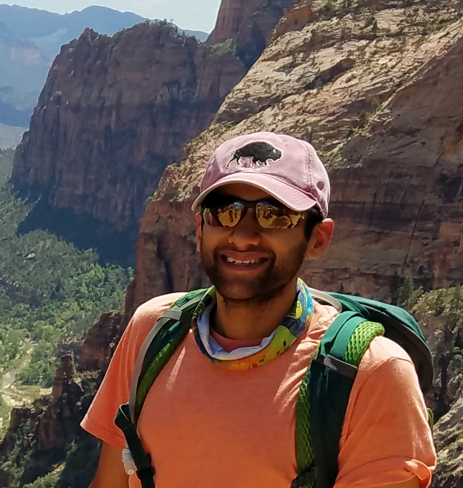
When I am not in the lab, I am usually outdoors. Running/climbing/backpacking and enjoying the beautiful pacific-northwest landscape.