Hybrid nanophotonic integration of solid-state defect qubits
Optically addressable defect qubits like nitrogen-vacancy centers in diamond can be utilized for quantum information processing.
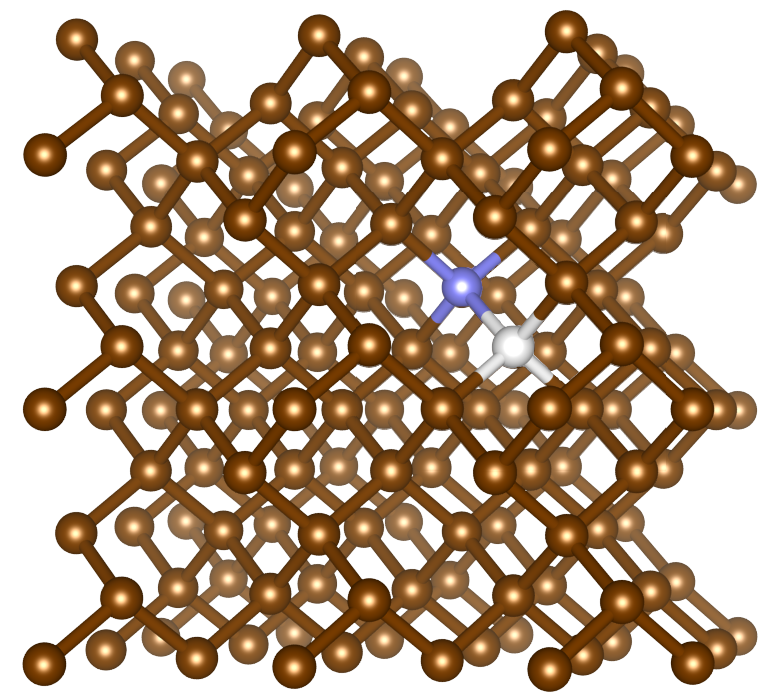
The nitrogen-vacancy (NV) center, a point defect in diamond (shown to the right), consists of a single nitrogen atom (purple) in a diamond lattice (brown) adjacent to a vacancy (white). NV centers offers long spin coherence time (>1 ms) along with the capability for high-fidelity optical initialization, spin readout and the possibility of coupling to in-situ long-lived quantum memories (13C nuclear spins).