Suspended BGaP-on-Si disk resonators (SEM) (Top-view)
Patterned with HSQ electron beam lithography using BGaP (220nm) on silicon substrate. The 5um dia. BGaP disks are undercut with a XeF2 vapor etch.
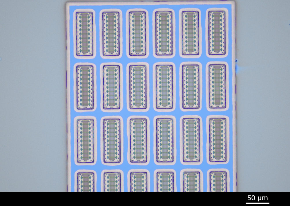
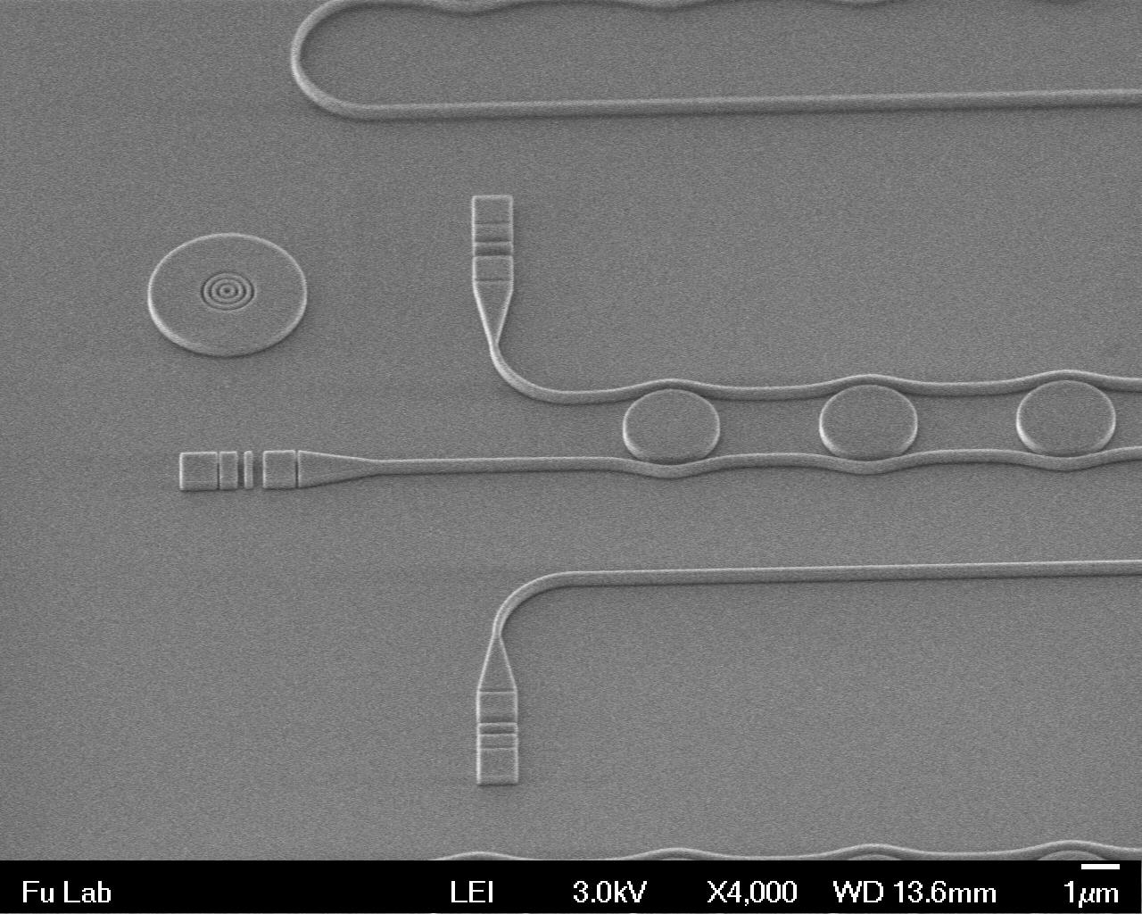
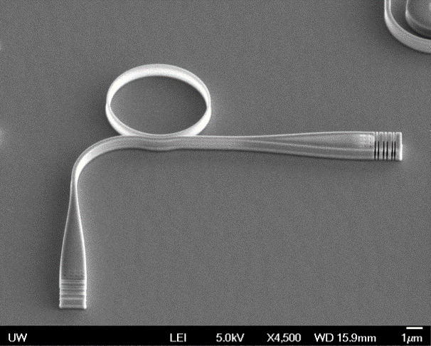
A collection of optical and scanning electron micrographs of hybrid photonic devices that I designed and fabricated at the WNF during my graduate studies.
I utilized electron beam lithography and RIE plasma etching processes to create devices with minimum feature sizes as small as 40 nm.
Patterned with HSQ electron beam lithography using BGaP (220nm) on silicon substrate. The 5um dia. BGaP disks are undercut with a XeF2 vapor etch.
Patterned on epitaxially grown BGaP (220nm) on silicon substrate. The 5um dia. BGaP disks are undercut with a XeF2 vapor etch.

Patterned on epitaxially grown BGaP (220nm) on silicon substrate. The 5um dia. BGaP disks are undercut with a XeF2 vapor etch.
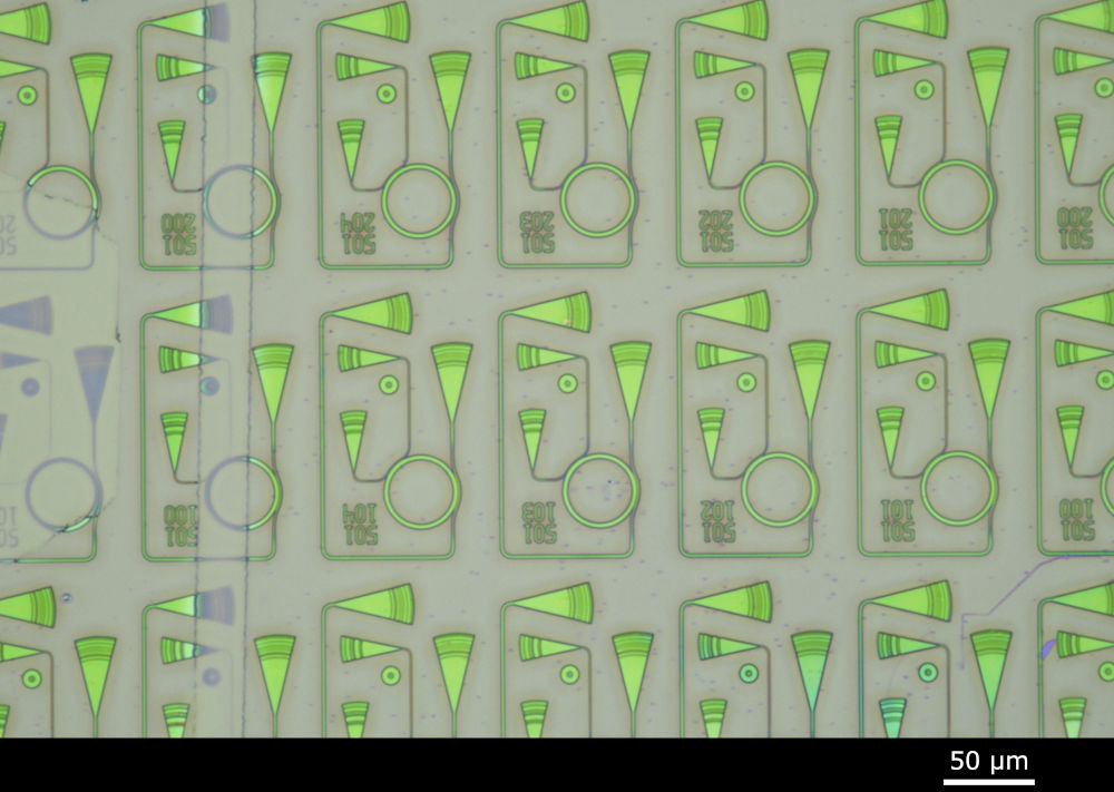
The suspend BGaP appears yellow and BGaP-on-Si is blue. The input and output gratings glow green. Each pair of gratings is connected by a photonic crystal waveguide.
The BGaP is patterned by E-Beam lithography and RIE plasma etching. The BGaP beams are released from the underlying Si substrate by a vapor etch XeF2 process.
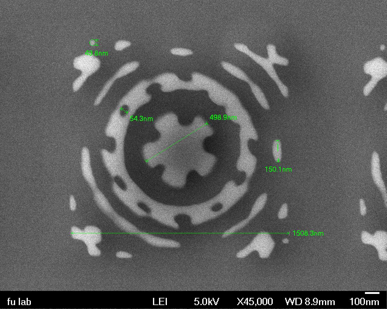
The devices are designed for stamp-transfer onto a diamond substrate that hosts solid-state qubits (silicon vacancy centers).Smallest hole size here is ~35nm.

Angled SEM emphasizes the large undercut beneath the 220nm thick BGaP photonic structures.

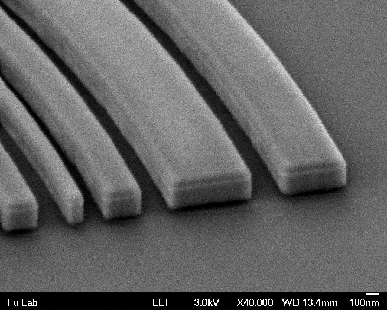
The beams are 220nm thick and 360nm wide.
The GaP devices (green) are fabricated on a silicon nitride substrate. The 250nm GaP membrane is wet transferred onto the nitride.

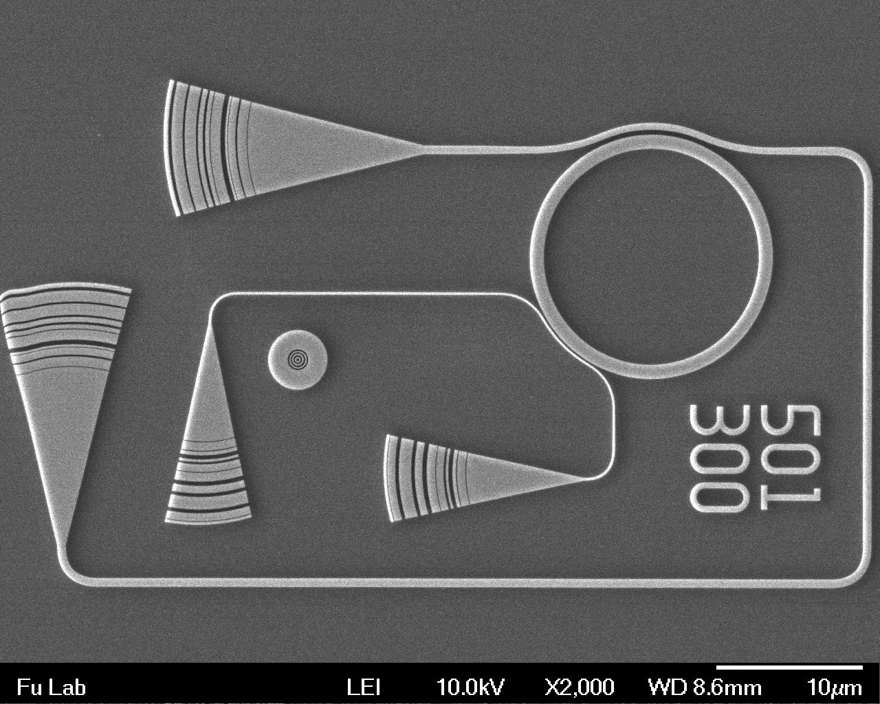
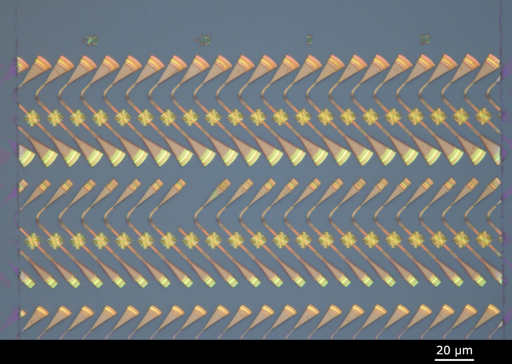
The two sets of gratings and coupling regions are designed for 1550nm (input) and 775nm (SHG output).

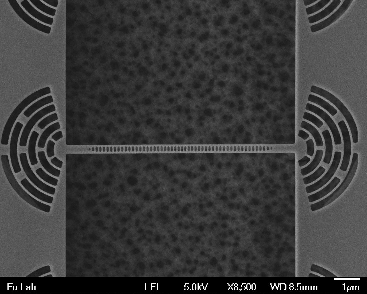
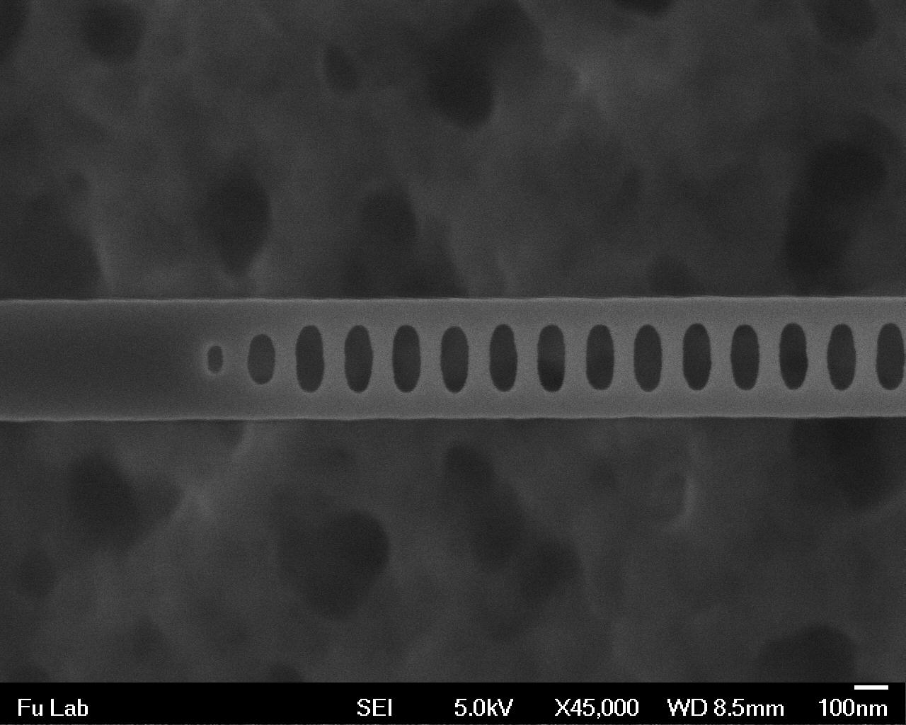
The gratings are connected by a small section of waveguide. These devices are designed for characterization of the grating transmission spectra. The narrowest slot in the grating has a width of 40nm.
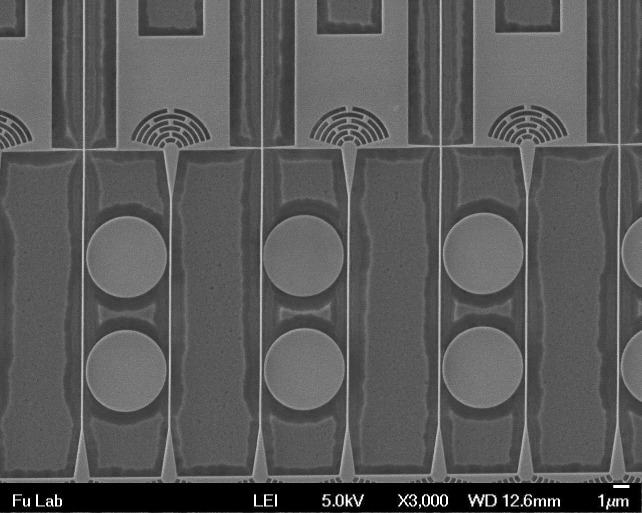
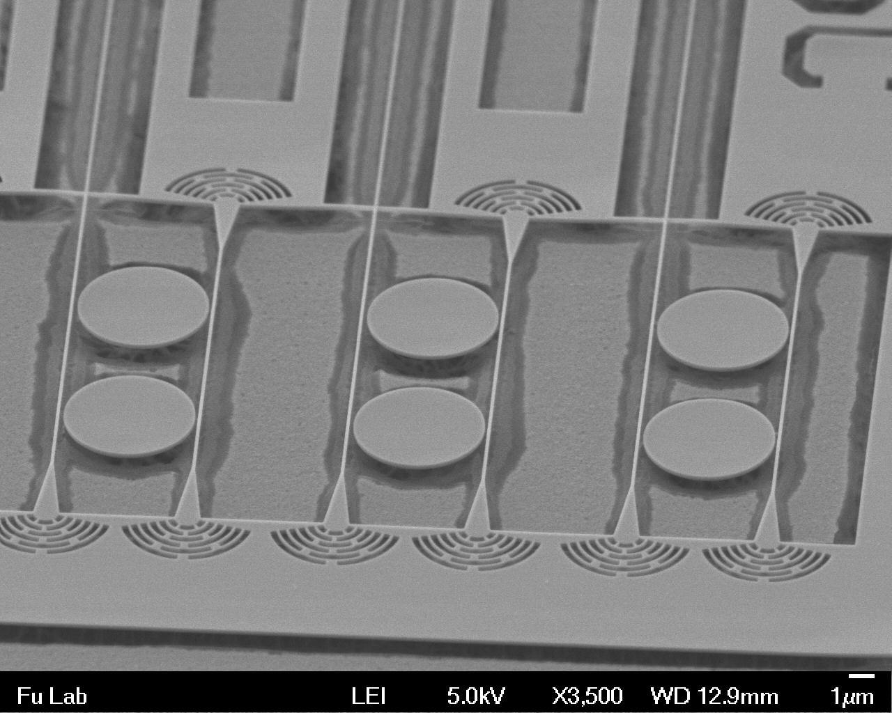
Disk resonators patterned with HSQ e-beam resist spun on a GaP-on-silicon nitride substrate. The 250nm GaP layer was transferred by wet liftoff from a GaP-on-AlGaP sample.

The smallest disks are 1um in diameter, with the waveguide-disk coupling separation ~100nm.

The input, drop and transmission grating couplers are shown etched into the GaP material (GaP-on-SiNx substrate). The smallest slot in the grating is ~60nm wide.
Devices are etched into GaP (GaP-on-SiNx substrate).

Devices are etched into GaP (GaP-on-SiNx substrate).

Inverse designed photon extractor patterned on HSQ e-beam resist spun on a GaP-on-diamond substrate. The 250nm GaP layer (yellow) was transferred by wet liftoff from a GaP-on-AlGaP sample.

RIE etching transfers the pattern into the GaP layer, without etching into the diamond substrate.

These photonic devices are evanescently coupled to single nitrogen-vacancy solid-state qubits ~100nm deep in the diamond substrate
The smallest features are 45nm diameter pillars.
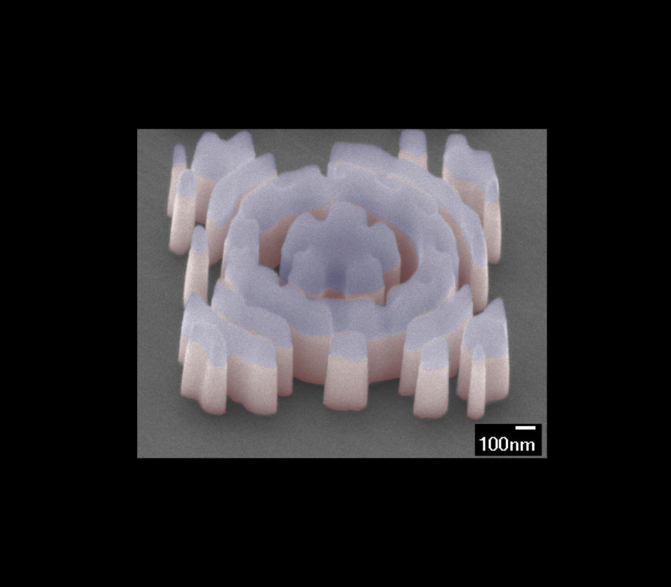
Layers: HSQ E-Beam resist (blue), GaP (pink), Diamond (grey)
Inverse designed resonators for second harmonic generation, patterned with HSQ e-beam resist spun on a GaP-on-oxide substrate. The 250nm GaP layer was transferred by wet liftoff from a GaP-on-AlGaP sample.
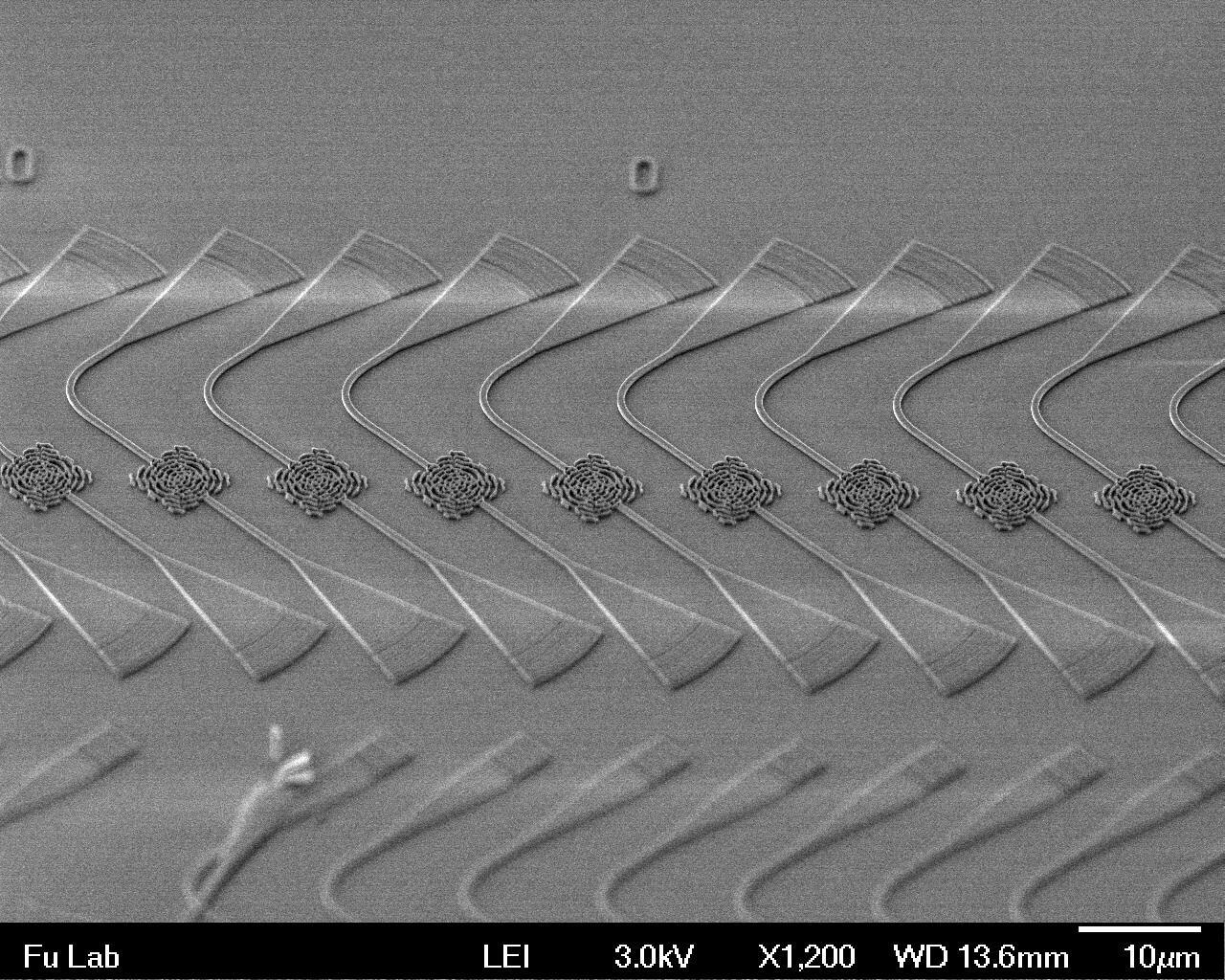
GaP-on-oxide inverse SHG photonic devices
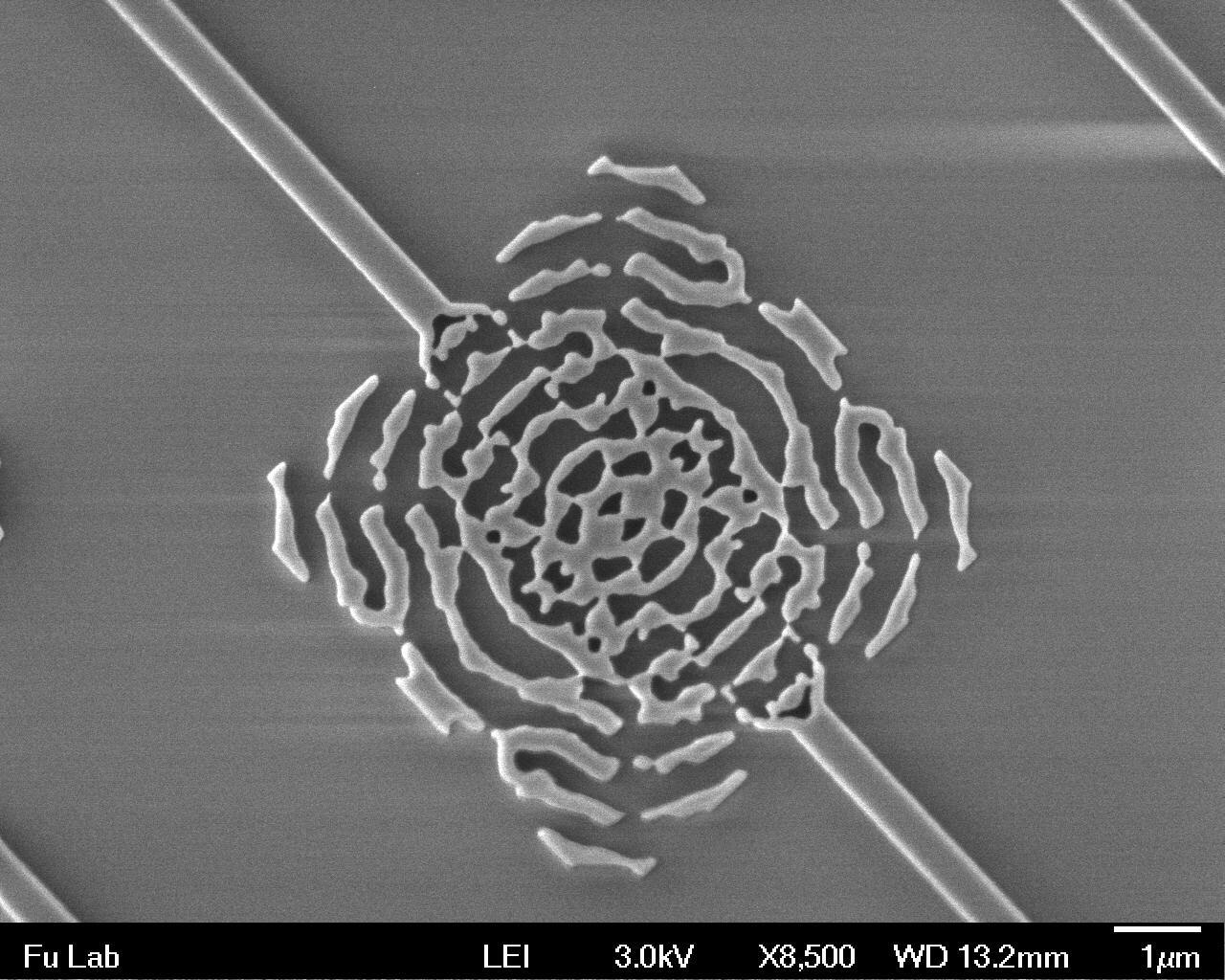
GaP-on-oxide inverse SHG photonic devices
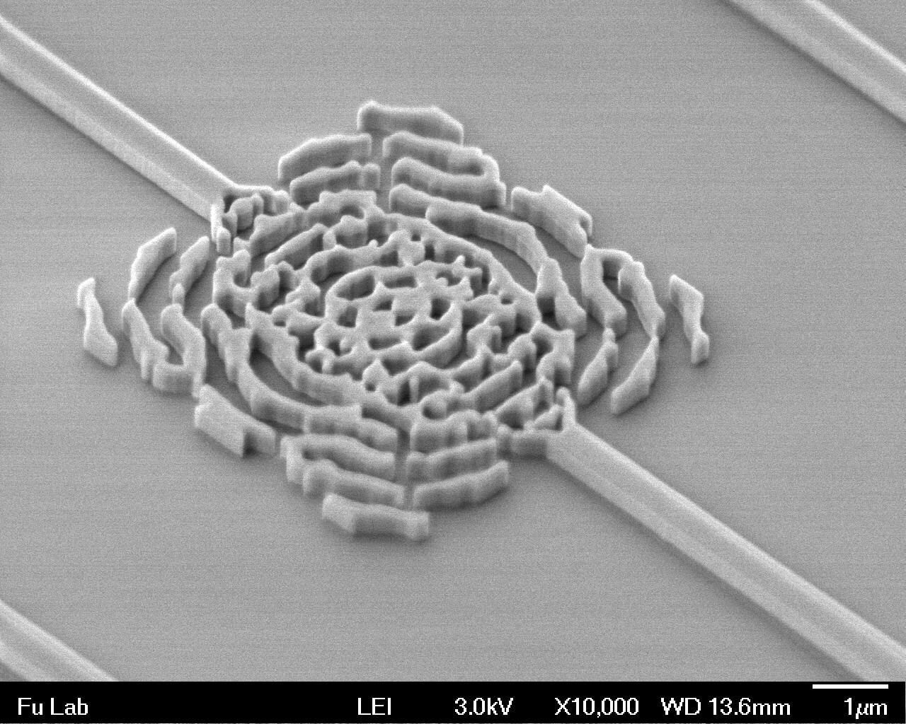
GaP-on-oxide inverse SHG photonic devices
The two layers are HSQ resist (top) and GaP (bottom) on a silicon oxide substrate
Patterned on epitaxially grown GaP (150nm) on AlGaP (400nm) on GaP substrate.

Patterned on epitaxially grown GaP (150nm) on AlGaP (400nm) on GaP substrate.
The different material layers (HSQ resist, GaP, AlGaP, GaP substrate) are visible. A custom RIE etch process (Ar\Cl2\N2) was developed for the high aspect ratio etched structures.
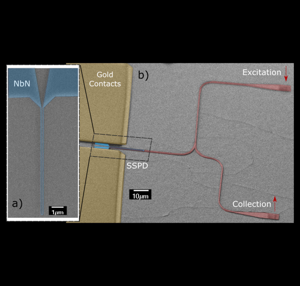
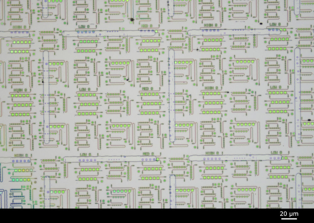
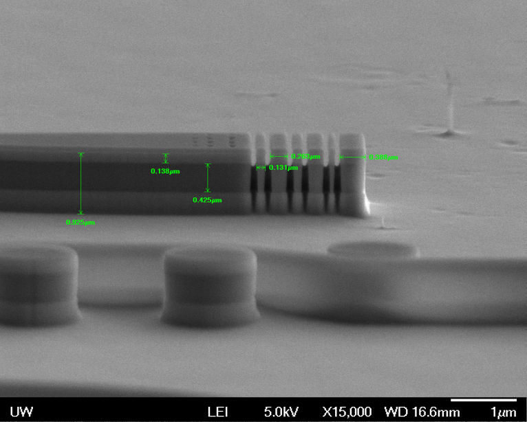
Layers (from top to bottom): Gold contacts (yellow), Niobium nitride (blue) superconducting nanowire, GaP waveguides(pink), AlGaP substrate (grey). The nanowires are 80nm wide and 6nm thick.